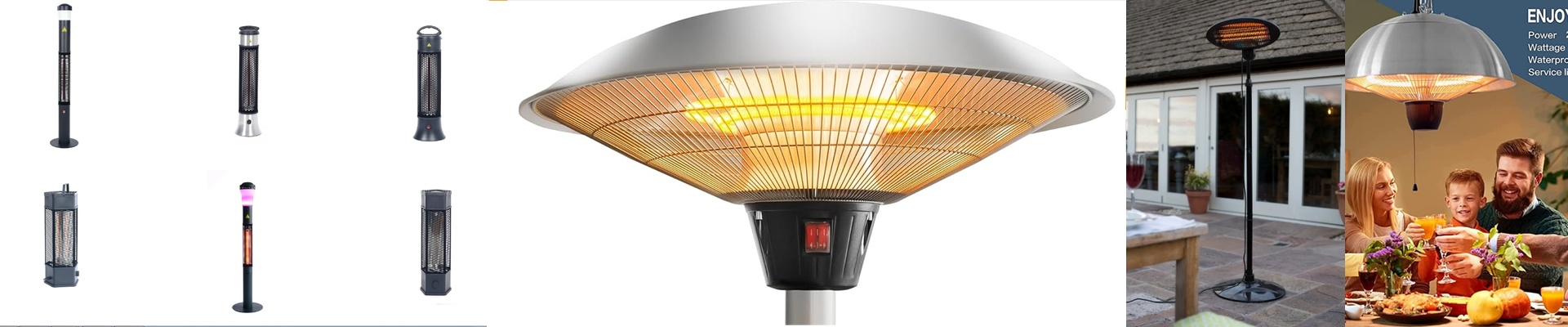
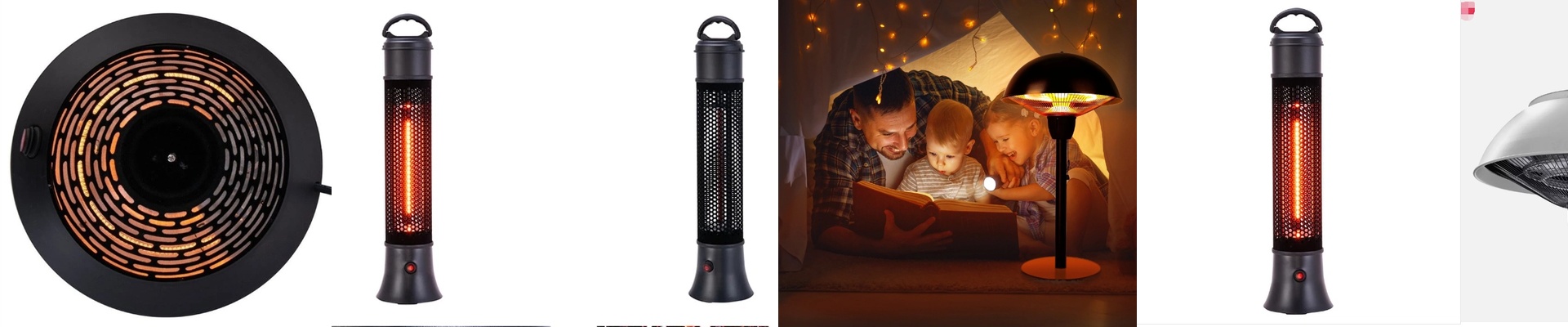
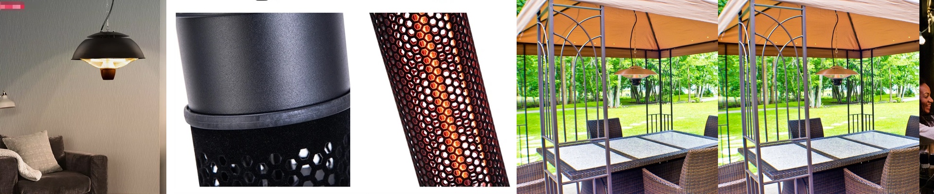

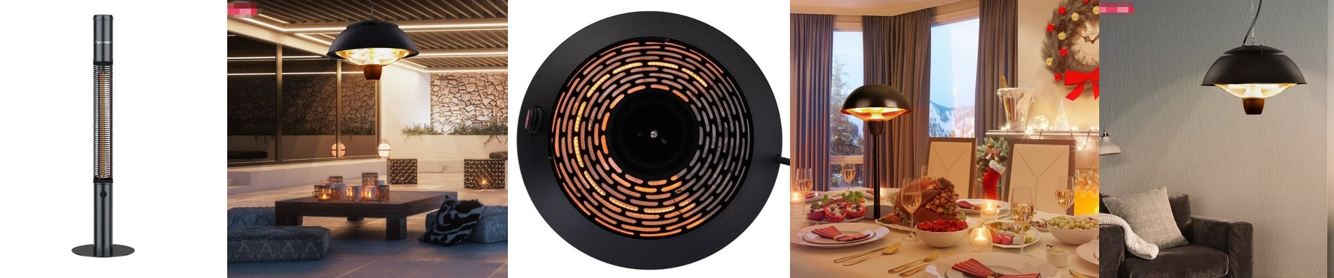
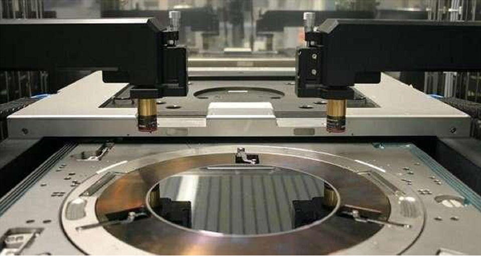
Out on the lithography floor, the wafer comes off the final rinse and the clock starts. Conventional drying leaves behind water marks, thin films, and particles you can’t see — until they show up as defects in the photoresist. In a 300mm fab running Class 1 cleanliness, that isn’t a risk. It’s yield walking out the door. What matters under the hood We built the wafer drying infrared heater around short-wave NIR. It dumps energy straight into the water film, fast — response under 50ms. Thermal uniformity across the wafer holds at ±0.1°C, so you don’t get hot/cold spots that mess with photoresist reflow after soft bake and hard bake. The emitter arrays sit behind sealed quartz, with a low-outgassing, particle-free interface, and the platform is cleanroom-compatible down to Class 1–100. Repeatability comes from closed-loop control that tracks setpoint within 0.5%, even running 24/7. In multi-cluster deployments, we’ve logged zero unplanned downtime over 18 months. Why this works where it counts Before spin, you need a truly dry wafer. After spin, you need bake profiles you can count on. The infrared heater dries without touching the surface, stripping the last 10–20nm of water without residues that cause scumming or bridging. The same thermal platform handles photoresist soft bake and hard bake with stable profiles, so linewidth control tightens and rework drops. Fewer defects. Less scrap. Cycle time you can plan around. Energy use falls because the heater delivers on-demand, without idling bulk fixtures. Installation needs clean alignment to the process chamber and a dedicated exhaust path to pull out latent solvents during bake. The heater plugs into SEMI-standard tool interfaces, though legacy platforms may need minor mechanical tweaks. Commissioning is short once you tune the recipe to your photoresist stack. In high-throughput lines, set up a schedule to inspect the quartz window — it keeps particle performance where it needs to be.